A division of Vishay Intertechnology, Inc.
CAD Data Guidelines
|
ATP has a talented team of CAD professionals to convert your CAD designs from specification control drawings (spec drawings) into the various documents needed for thin-film processing. To facilitate these documents, we request that you incorporate the following information and design guidelines in your CAD package so that we may accurately process your design: 1. Purpose1.1. The purpose of these guidelines is to help insure on time delivery and that each order will be built to specification. |
||||||||||
2. Scope2.1. This reference identifies simple CAD rules and methods that will communicate the design. 2.1.1. Note, some of the information below is specific to CAD software. |
||||||||||
3. Referenced Documents3.1. N/A |
||||||||||
4. ATP TemplateAvailable on request. |

ATP Template |
|||||||||
5. Data Guidelines5.1. Please refer to ATP’s design guidelines and catalog specifications. 5.2. Provide CAD data scaled in inches. 5.3. Please do not provide CAD data all on one layer. Figure One shows a design that is all on one layer and one color. This is not clear and may be interpreted incorrectly. 5.4. Figure Two is clearer than Figure One. In Figure Two, each component of the design has been identified by color and layer. See below.
5.5. Figure Three (Preferred) is the same as Figure two, except the metallized, areas (resistor and gold) have been clearly identified by a “hatch” pattern. This is very helpful. |

Figure One 
Figure Two 
Figure Three |
|||||||||
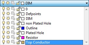
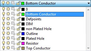
6. Data Guidelines Two-Sided (Double-Sided) Circuit6.1. Double-sided circuits have patterns on the top and bottom sides. 6.2. Figure Four clearly identifies the top and bottom patterns. See below the screen shot of the added bottom layer to help identify the CAD Data.
6.3. Figure Five is Through View. This CAD data helps the CAD Drafter understand the bottom orientation relative to the top when via holes are not present or the design is not symmetric. |

Figure Four 
Figure Five |
|||||||||
7. Annotation Guidelines7.1. This section is provided to help the designer annotate a drawing. Do not over-dimension. Circuit patterns will come from the data provided to Cad. Provide a tolerance only if required for the design. Refer to Figure Six. All dimensions in Inches [mm]. |

Figure Six |
|||||||||
8. CAD Guidelines8.1. Refer to Figure Seven. Draw all patterns using closed joined polylines. All polylines should be zero width. 8.2. Draw in Model Space. No Circuit Data or Circuit layers in Paper Space.
8.3. Notes and dimensions in Paper Space are fine. 8.4. No Xrefs, No Elevation or Thickness. Please do not use Splines, Ellipses or Regions. |

Figure Seven |
|||||||||
9. Substrate Array(Arrayed CAD Data is not required. This is optional.) 9.1. All Dimensions are in Inches [mm]. 9.2. Use Figure Eight and Figure Nine as a reference for preparing and arraying data onto a substrate. 9.3. The example shows how to array a circuit on to a 2"x2" Substrate using a .010" Dicing Kerf (Saw Street). 9.4. Figure Eight shows how Dicing Marks and the array are created in CAD. This is the simplest and most accurate method. 9.5. Additional ARRAY information. 9.5.1. The mask array determines the substrate that can be used. The size of the substrate used heavily influences the final cost of the circuit. The array size depends on the circuit size and the quantity ordered. When ATP fabricates the mask, the optimum array size will be determined for you. Creating arrayed data is optional, but if you are providing arrayed data it should be arrayed on the substrate size optimal to the number of circuits (and size) required. Please contact ATP Sales to determine the optimum array size. Standard array sizes are 1" x 1" (25.4mmX25.4mm), 2" x 2"(50.8mmx50.8mm), 2.25" x 2.25" (57.2mmx57.2mm), 3.25" x 3.25" (82.6mmx82.6mm) and 4" x 4" (101.6mmx101.6mm). Mask Glass Size will be determined by ATP. 9.5.2. The standard border (keep out) size from the outside edge of the substrate is 0.050" (1270um). 9.5.3. The stepping distance of the circuits in the array is determined by adding the dicing kerf to the circuit size. The dicing mark must be centered as shown in Figures Eight and Nine. 9.5.4. Figure Ten is an example of a Multi-circuit array (pizza). Follow all the preceding guidelines in section 9.5 and add the quantities of each circuit part number as shown in Figure Ten. |

Figure Eight 
Figure Nine 
Figure Ten |
|||||||||
10. Adding Circuit Text10.1. Upon request, ATP can supply our customer with down-loadable AutoCAD Text that can be used in the data that will be supplied to ATP. This text is made of “closed joined polylines” and was created to work with our processing. 10.2. This text can be used to make any part number or text required on a circuit. 10.3. Below is a screenshot of the AutoCAD text available from ATP: 10.3.1. Dimensions are in Inches [mm]. |

Letters and Numbers Sizing |
|||||||||
Note Any changes to a drawing or CAD file after submission of a quote, will require a revision change and request for a re-quote. |
||||||||||