Laser Diode Submounts (Au/Sn)

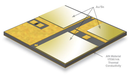
Applied Thin-Film Products (ATP) is one of the industry leaders for Laser Diode Submounts with pre-deposited Au/Sn. ATP custom fabricates thin-film submounts with tightly controlled substrate and metal thicknesses for your alignment needs. Hi-thermal conductivity materials include Aluminum Nitride (AlN) and Beryllium Oxide (BeO).

These submounts can have pre-deposited and patterned Gold Tin (Au/Sn) to accommodate lower manufacturing cost, higher volume, and automated assembly of laser diode modules. The use of pre-deposited and patterned Au/Sn replaces the more traditional approach of using thick Au/Sn preforms. ATP’s standard alloy composition is 80% Au and 20% Sn which typically reflows at 278°C under a high purity gas blanket consisting either of forming gas or Nitrogen.

Other Au/Sn custom compositions are available. ATP offers a sputtered and plated Au/Sn eutectic. Samples are available. Please ask for ATP1014S for sputtered, ATP1014P for plated and ATP1014PX for advanced plated AuSn.

In order to strengthen the relationship with our customers, ATP performs Au/Sn reflow tests as a standard practice on each lot to ensure the performance of the Au/Sn meets our customers’ expectation. We offer four standard test profiles for our customers to choose from that would closely resemble their assembly processes:

  Laser Diode Submount

Laser Diode Submount

Test Profile Profile Detail Placement of test die on Au/Sn Pattern Scrub On/Off Station Note Program Number
1
{Standard}

Circuit with Au/Sn pattern is
placed on work holder which is
at 290–305°C for 5 seconds

After the circuit with Au/Sn pattern is placed on work holder On Non-programmable See “AuSn Customer listing” on Master History List. No program number
2

260°C ± 5°C soak for 1 min

Ramp to 290–305°C and stay
for 5 seconds

As the beginning of the soak and the test die is held down until completion of the profile Off Programmable See “AuSn Customer listing” on Master History List. 1
3

200°C ± 5°C soak for 2 seconds

Ramp to 290–305°C and stay
for 5 seconds

After ramp temparature is reached On Programmable See “AuSn Customer listing” on Master History List. 2
4

Start at 160°C

Ramp to 330°C ±5°C and stay
for 8 seconds

At the beginning of the soak and the test die is held down until completion of the profile Off Programmable See “AuSn Customer listing” on Master History List. 3


Notes: Test Profile 1 is typically recommended for sputtered Au/Sn patterns.
Test Profile 1 is applicable to both plated and sputtered Au/Sn patterns. Test Profiles 2 and 3 are only applicable to plated Au/Sn patterns.
All test were performed at ATP with inert gas.

Custom test profile and the detailed test procedure are available upon request. Die Shear test will be performed on the test die to meet and/or exceed MIL-STD-883.

Replaces Traditional Au/Sn Preforms

Accurately Controlled Thickness

Lot to Lot Consistency

Reduce Au/Sn Thickness

Complex Solder Pad Geometries

Accurate Laser Alignment

Pre-Deposited and Patterned Au/Sn Guidelines

Smallest Feature Size: 0.0015" x 0.0015" (0.038mm x 0.038 mm)

Minimum Pitch (minimum space between Au/Sn Pads): 0.003" (0.076mm)

Typical Au/Sn Thickness: 160–240µ" (4–6 microns) (Thickness outside of the typical range might restrict the process used.)

AuSn thickness with 3–6µm for sputtered and 4–7µm for plated

Tolerance on Thickness of Plated Au/Sn: ±80µ" (±2 microns)

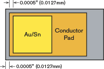
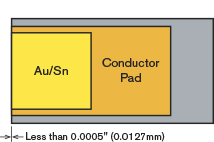
Placement Accuracy of Au/Sn: ±0.0005" (±0.0127mm)

Dimensional Tolerance on Au/Sn Pad: ±0.0002" (±0.005mm)

Minimum Pull Back From Laser Cut Edge: 0.0015" (0.0381mm)

Minimum Pull Back From Conductive Plated Thru Via Holes: 0.0025" (0.0635mm)


ATP circuits with Au/Sn are best assembled when received. Little information is available about long-term storage of thin Au/Sn layers under ambient conditions. Gold Tin intermetallic compounds (IMCs) are known to form at room temperature when excess Au or Sn is present, so compositional changes might occur during long-term storage. To our knowledge, oxidation of Au/Sn IMCs has not been studied but likely is accelerated by high humidity and high storage temperature. Storing the circuits with Au/Sn in a nitrogen purged dessicator may minimize the oxidation effect.

 
Typical

Typical

  Select

Select

ATP1014P: Plated after reflow

ATP1014P: Plated before areflow

 
ATP1014P: Plated after reflow

ATP1014P: Plated after reflow

ATP1014S: Sputtered before reflow

ATP1014S: Sputtered before reflow

ATP1014S: Sputtered after reflow

ATP1014S: Sputtered after reflow

Company Technologies Capabilities Design Guidelines Products Other

Introduction

Polyimide Bridges

Photomasks

Standard Dimensions, Tolerances

Inductor Coils

Home

Quality Assurance

Solder Dams

Substrates

CAD Data Guidelines

Inductor Coils Eng. Kit

Contact Us

Directions

Laser Diode Submounts

Material Specifications

Material and Conversion Tables

Microstrip Transmission Lines

Careers

Careers

Vias: Plated Through

Ion Beam

Thermal Performance

Transmission Lines Eng. Kits

Terms of Use

Sales Rep’s

Vias: Au or Cu Solid Filled

Aluminum Bonding Pads

Aging Equation

Stand Off/Isolation Pads

Privacy Policy

Contact Us

Edge Wraps

Laser Machining/Drilling

Safe Current Limits

ATP Bond Qualification Coupons

Facebook


Gold Bumping

Backside Burnishing

Design Resources

Product Samples

YouTube


Fractal Fasten

Standard Metallizations


Packaging/Chip Trays


Integrated TaN Resistors


Thin Film Resistor and Multi-Tap


Laser Resistor Trimming


Serialization