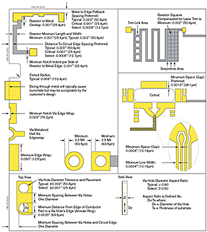
Standard Dimensions and Tolerances
ConductorsAu: Minimum Line-Width (Trace) Typical: 0.0004" (10.16µm) for <200µ" thick. Contact ATP Sales for smaller dimensions. Au: Minimum Gap (Space) Typical: 0.0004" (10.16µm) for <200µ" thick. Contact ATP Sales for minimum gap for etchback. Cu: Minimum Line-Width (Trace) Typical: 0.0004" (10.16µm) for <200µ" thick. Contact ATP Sales for Cu >200µ" thick. Cu: Minimum Gap (Space) Typical: 0.0004" (10.16µm) for <200µ" thick. Contact ATP Sales for Cu >200µ" thick. Cu or Au: Maximum Thickness Maximum: 0.002" (50.8µm) Contact ATP Sales for details.
TolerancesAu: Dimensional Tolerance on Critical Areas Typical: ±0.0002" (5.08µm) Critical: ±0.0001" (2.54µm) Select: ±0.00005" (1.27µm) Dimensional tolerance on non-critical areas: Cu or Au: Dimensional Tolerance on Critical Areas Where Cu is Thicker Than 0.0005" (500µ") or (12.7µm) Typical: ±0.0003" (7.62µm) Select: ±0.0002" (5.08µm) Dimensional tolerance on non-critical areas: Typical: ±0.0004" (10.16µm)
ResistorsResistor Minimum Length and Width Minimum: 0.001" (25.4µm) Typical: 0.002" (50.8µm) Contact ATP Sales for dimensions which will require a relaxed tolerance. Resistor Tolerance (With Laser Trim) Typical: ±2.0% Select: ±0.5% Select is dependent on size of resistor.
Vias - HollowVia Hole Diameter Aspect Ratio Typical: ≥ 0.80 Select: > 0.50 Aspect ratio is defined as: Dv / Ts where: Dv = Diameter of the via (thru hole) Ts = Thickness of the substrate Via Hole Diameter Tolerance Typical: ±0.002" (50.8µm) Select: ±0.001" (25.4µm) Via Hole Location Tolerance Typical: ±0.002" (50.8µm) Select: ±0.001" (25.4µm) Via Hole Taper Typical: 10% Select: ±0.001" (25.4µm) Via Hole Spacing (Hollow Plated) One diameter minimum distance Via Hole Proximity to Edge of Circuit One diameter minimum distance away from edge Via to Pattern Registration (Hollow Plated) Typical: ±0.002" (50.8µm) Select: ±0.0005" (12.7µm) Contact ATP Sales for details. Front to Back Image Registration Typical: ±0.001" (25.4µm) Select: ±0.0005" (12.7µm) For Solid Filled Vias see |
LaserLaser Machined Features Typical: ±0.002" (50.8µm) Select: ±0.001" (25.4µm) Metal Pullback From Laser Features Front side: Typical: 0.002" ±0.002" (50.8µm ±50.8µm) Select: 0.001" ±0.001" (25.4µm ±25.4µm) Backside: Typical: 0.003" ±0.003" (76.2µm ±76.2µm) Select: 0.002" ±0.002" (50.8µm ±50.8µm) Laser Machined Features Next to Au/Sn Minimum distance: 0.005" (127µm) for Al2O3 Minimum distance: 0.010" (254µm) for BeO Laser Machined Radius Typical: 0.006" (152.4µm) Select: 0.003" (76.2µm)
DicingCircuit Dimensional Tolerance — Diamond Sawn Typical: ±0.002" (50.8µm) Critical: ±0.001" (25.4µm) Select: ±0.0005" (12.7µm) Via Trench Cut Depth Tolerance Typical: ±0.002" (50.8µm) Dicing through metals will typically cause burrs/tails and on polished materials could affect adhesion. Another solution ATP recommends to prevent these type of issues is by putting a pullback typical .001" (0.0254mm) in the design of the circuit. Contact ATP Sales for more information. Diamond sawing (dicing), scribing, or breaking of cut thru edge vias or castellations may cause undercutting or separation induced anomalies. If it is required by design, then ATP will refer and adhere to MIL-STD-883J Section 3.1.1.3.
Notes and RecommendationsNote: For long term storage, ATP recommends storing thin-film circuits ideally at room temperature in a nitrogen purged dessicator (or equivalent) and using a pre-clean method that is compatible with thin-film circuits prior to assembly. Note: ATP is a fabricator of custom thin-film circuits and does not claim to be an electrical design consultant. ATP does not guarantee electrical performance of any customer supplied custom designs. Note: All thin-film circuits shipped from ATP are free of debris and FOD when packaged. However, alumina and other hard substrate materials have very sharp corners and edges that can act like knife edges and may create debris and FOD from the packaging materials used during the shipping process. Some large and unusually shaped circuits may require a special foam insert to ensure breakage does not happen during shipping. ATP makes every effort to ship clean and QC approved thin-film circuits but it is for these reasons ATP recommends using a pre-clean method that is compatible with thin-film circuits prior to assembly. |
Design Guideline Dimensions and Tolerances
Download the “ATP Design Guideline Dimensions and Tolerances Illustration” in PDF format.* For more information on dimension and tolerances, please request document #DG50020 “Design For Manufacturability,” in PDF format.* *PDF documents require Adobe Reader. |
||||||||

