Laser Machining/Drilling
|
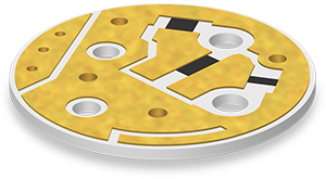
Our computer-controlled lasers can create features of virtually any planar shape and can deliver positional accuracies of 0.001" (0.0254mm) or better over areas as large as 8"x8" (203.2mm x 203.2mm). The laser is extremely flexible and permits close location of features with considerable layout flexibility. |

Burnished Treatment 
Dual Beam Lasers |
|||||||||||||||||||||||||||||||||||||||||
Types of Ceramic MaterialsMaterials covered include Alumina, Beryllium Oxide, Aluminum Nitride, Ferrite and Fused Silica/Quartz. Machined Features/Special Shapes

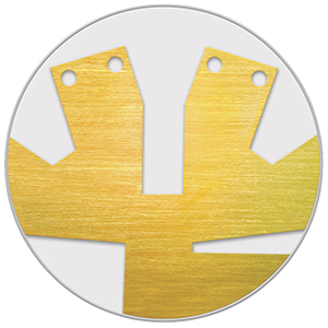
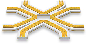
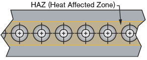
Virtually any planar shape can be cut in ceramic substrates. These shapes include circles, curves, rectangles, polygons, rounded thin slots, etc. Since ceramics are strong but brittle, the designer should consider a radius as large as practical on the inside corners. All inside corners will need to have a minimum of 0.003" (0.0762mm) radius due to the laser beam diameter. Rounding inside corners can reduce chipping and cracking. Laser machining next to conductor lines should be pulled back from edge by 0.001" or 0.0254mm minimum. Minimum cut slot width: 0.004" Corner radius: 0.004" typ. HAZ is presented when laser drilling is involved. |
Backside Burnishing TreatmentATP continues to offer a backside burnishing treatment that will minimize burrs, tails and post laser slags on the backside of substrates. This treatment can be used when laser cutting through gold on backsides of substrates. This cost effective process could also improve adhesion and eliminate the need for customers to “roughen up” the surface of the components themselves before epoxy bonding. Backside burnishing treatment should not be confused with ATP’s Fractal Fasten technology, see Fractal Fasten technology page. Please contact ATP Sales for further information on the Backside Burnishing Treatment. AnnealingHigh temperature annealing for Alumina-based substrates is also offered. This can increase ceramic flexural strength, improve adhesion and reduce internal stresses. Handling and CleaningLaser protective coating is applied to protect material surface finishes and parts during the laser process. Laser protective coating also guards against adhesion of “slag” to material surfaces. Slag buildup is primarily found on the beam exit side of the substrate and is removed after laser processing. 
Top View |
|||||||||||||||||||||||||||||||||||||||||
|
|
||||||||||||||||||||||||||||||||||||||||||
Tolerances for Machining/DrillingATP’s standard validation method for Machined/Drilled features is from the topside, prior to any metallization being applied. If a validation method is not specified, ATP will default to ATP’s standard topside validation process for Machined/Drilled features. Other taper and diameter tolerances available upon request. Please contact ATP Sales for more information. |
|
|||||||||||||||||||||||||||||||||||||||||

