|
Two issues will be discussed in the following:
•Electromigration
•Joule heating
Electromigration
Earliest workers in thin-film microelectronics observed that a large, steady electrical current could cause voids to form in thin-film Aluminum and Gold traces, ultimately causing the trace to fail. Raising a trace’s temperature caused it to fail at even lower currents. Such electromigration failures were far less likely if RF currents of the same amplitude were used.
Experiments showed large differences in electromigration threshold that depended on the grain structure of the metal trace. Copper (Cu) generally was found to be more resistant to electromigration than Gold (Au). Discussion of some of these variables can be found in the references 1 and 2, listed below.
However, for both Au and Cu, a current density of 105 A / cm2 appears to be safe at usual operating temperatures of hybrid microelectronics. Thus in the following discussion, we will assume that the maximum acceptable current density is given by:
Jm = 1.0 x 10⁵ Amps / cm2
Equation 1
Im = Jm t W = t W x 105 Amps.
Equation 2
Joule Heating
Do such large currents cause significant Joule heating in the traces? The short answer is: Yes! Power dissipated in the trace is given by the following expression:
P = I2 R = ρ J2 WLt (Watts)
Equation 3
The thermal flux that the substrate must conduct away from the trace becomes:
Q = P / (WL) = ρ J2 t (Watts / cm2)
Equation 4
Q depends only on the metal’s electrical resistivity, the square of the current density and the trace’s thickness. The thicker the trace — with the current density fixed at Jm — the more power that must be conducted away from the trace!
NOTE: This problem is not the same as determining the fusing current of a free-standing bond wire!
|
|
Design Tools
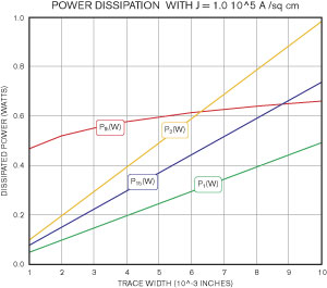
Figure 1 shows a plot of Eqn 3), power dissipated in a 0.100" (2.54mm) long Cu trace versus trace width, W, for 0.001" (0.025mm), 0.0015" (0.038mm) and 0.002" (0.051mm) thick plated Cu traces. The assumed electrical resistivity of the Cu-plating was 3.0 x 10⁻⁸ Ω-m.
Thermal Model
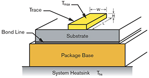
The upper-most trace on the left in Figure 1 is an empirically-derived thermal limit for a 0.010" (0.254mm) thick 99.6% Alumina substrate epoxied to a Kovar carrier and secured to an Aluminum heatsink. The heatsink temperature was set at 85°C with the maximum trace temperature of 100°C, a 15°C temperature rise due to the Joule heating. Due to AlN and BeO substrates’ high thermal conductivities, their thermal limits are far too high to have a practical impact.
How to Use This Graph
•If your substrate is AlN or BeO, then you do not need to worry about Joule heating. The thermal limits for these substrate materials are much too high to impact your design.
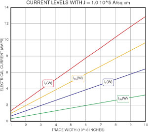
•If your substrate choice is Alumina, then go to Figure 2, a plot of current versus trace width, W, for 0.0005" (0.0127mm), 0.001" (0.0254mm), 0.0015" (0.038mm) and 0.002" (0.051mm) trace thicknesses. Decide on a trace width and thickness for your bias line.
•Return to Figure 1 to make sure that your choice of trace dimensions does not lie above the thermal limit (upper-most trace on the left side).
•If the dissipated power for your choice of trace dimensions exceeds the thermal limit, then you should evaluate the assumptions on which it was based for its relevance to your design (See Figure 3 and the Thermal Model paragraph above.)
These Design Guidelines are intended to assist you in choosing a safe bias current level. Can you exceed the limits on current density and temperature rise? Probably, but there is no simple answer to this question. Too many variables affect the electromigration wearout of thin-film metal traces.
References
1. Ryu, Changsup, et. al., Electromigration of Submicron Damascene Copper Interconnects, 1998 Symposium on VLSI Technology, June 8-11, 1998.
2. Kilgore, Steve, et. al., Electromigration of Electroplated Gold Interconnects, Mater. Res. Soc. Symp. Proc. Vol. 863 (2005).
|
|

Figure 1: Power dissipated in a 0.100" (2.54mm) long plated Cu trace versus trace width. The trace is on a yet unspecified ceramic substrate. The electrical current density in the trace is fixed at 1.0 x 10⁵ A/cm2. Also plotted is empirically-derived thermal limit for 10 mil thick alumina.

Figure 2: Graph of electrical current for a current density of 1.0 x 10⁵ A/cm2. Trace thicknesses of 0.0005" (0.0127mm), 0.001" (0.0254mm), 0.0015" (0.0381mm) and 0.002" (0.0508mm) are shown.

Figure 3: Cutaway view of thin-film metal trace thermal model.
|


